What you'll learn:
- 将CTSD技术应用于信号链设计。
- CTSD转换器比离散时间ADC的优点。
CTSD拓扑为优化传统体系结构以外的信号链提供了可能性。当今的许多应用程序都需要较小的形式,但仍需要相同的性能。开发人员经常面临如何实现这一目标并经常通过妥协做出的问题。
例如,可以通过牺牲噪声性能或准确性来减少外形。本文使用连续的Sigma-Delta(CTSD)转换器探索,作为优化设计并降低材料清单(BOM)成本和外形尺寸的新方法。
优化设计
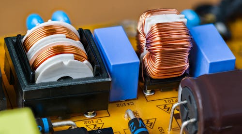
为了获得所需的传感器或信号的最佳产率,信号链中的所有元素都必须完美协调。通常使用几个离散组件,从传感器到模数转换器(ADC)。除了传感器和ADC外,通常还有仪器放大器,ADC驱动程序,参考缓冲区和过滤器。选择合适的ADC驱动程序和滤波器设计,特别是代表了反复低估的错误源。
One way to optimize the design and reduce BOM costs as well as form factor is to use μModule devices. These devices are highly integrated solutions containing the converter as well as buffers and passive components. With this new CTSD technology, it’s possible to drive the ADC directly without having to use an amplifier as a buffer. In addition, the new topology allows for simplification of the filter design.
DT-ADC与CTSD转换器
图1显示了传统的离散时间ADC(DT-ADC)和CTSD转换器之间的差异。与传统设计相比,CTSD设计可将高达68%的外形降低。
使用开关电容器拓扑,例如SAR ADC或Sigma-Delta ADC等传统的DT-ADC。这是在ADC和参考输入上找到的。在两个阶段“样本”和“保持”之间进行差异。它们对应于“持有”电容器的充电和排放。因此,必须有足够的电流来充电和排放以及由于寄生性能引起的电荷吸收(电荷注入回扣)(图2)。
许多传感器无法提供如此高的电流,因此需要缓冲。除此功能外,驱动程序必须足够快(短时间安装时间,高振动率)才能在“样本”阶段结束时输出(图2C)要解决,以便没有将其他错误引入所需的信号中。因此,对ADC驱动程序的要求很高。
CTSD转换器具有电阻输入,可以直接由传感器驱动。如果传感器无法驱动ADC(例如,如果传感器具有很高的阻抗),则可以将简单的放大器插入以进行阻抗转换。
CTSD的另一个优点是固有的抗质量过滤器(低通滤波器)属性。使用传统拓扑,输入需要低通滤波器来过滤不必要的高频信号。
原因是奈奎斯特准则、范围h states that the sampling rate must be at least twice as high as the frequency of the desired signal. If the sampling rate is too low, aliasing may occur and undesired noise may fold over into the signal. One explanation for the inherent antialiasing filter properties of CTSD converters is that the sampling doesn’t occur right at the modulator input, but rather after the循环过滤器。
结论
CTSD拓扑除了优化信号链的传统体系结构外,还提供了另一种新的可能性。如果上市,bom或formage也起着重要作用,那么ADC等ADCAD4134represent good alternatives. Thanks to their resistive inputs and inherent filter properties, numerous designs can be simplified and optimized with them. In many applications, ADC drivers, passive components for the filter design, and reference buffers can be eliminated.