Last year, a new class of networking chip called the infrastructure processing unit (IPU) joined英特尔的服务器芯片的投资组合。现在,该公司正在对IPU进行长期赌注,因为它看起来像云巨人队赢得了青睐。
这家总部位于加利福尼亚州圣克拉拉的公司最近透露了IPU的路线图,该路线图持续到2026年,它建立在与Google共同开发的第一代IPU上。英特尔表示,它将继续根据两个FPGA客户可以随意重新编程以及将功能锁定在硬件中的ASIC以牺牲灵活性为代价的ASIC。每个新的IPU都会比最后一个更大的吞吐量 - 到2025年或更高版本,到800 GB/S以太网。
英特尔的foray into IPUs follows rival efforts by the likes of Marvell, NVIDIA, and pre-AMD Xilinx, which sell what they call the data processing unit (DPU) to offload infrastructure jobs that drag on the central (CPUs) and graphics processing units (GPUs) in a modern data center.
An IPU is fundamentally the same concept as a DPU. The goal is to free up a server’s CPU by intelligently offloading lots of networking-related and other backstage workloads to purpose-built protocol accelerators.
英特尔数据平台业务部门的副总裁和以太网产品的总经理Patty Kummrow在从云中的数据中心到边缘设备的所有内容中都看到了对IPU和其他特定领域特定处理器的需求。
Building Blocks
“IPU is a key part of the future data center architecture,” Kummrow said earlier this month in a briefing with reporters.
Today, the general-purpose CPU at the heart of a server acts as a traffic cop for the data center, managing networking, storage virtualization, encryption, and other security work that primarily runs on software today.
但是,依靠CPU来协调数据中心的流量是昂贵且效率低下的。根据NVIDIA的说法,在服务器中,CPU的能力中有超过三分之一在这些基础设施工作量上浪费了。
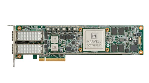
英特尔以网络卡的形式提供IPU,云公司可以将其附加到每个服务器上。IPU具有足够的处理功率,可卸载广泛的网络(RDMA上的RDMA或ROCE或ROCE),存储(非挥发性内存Express或NVME)和安全性(IPSEC)工作负载,这些工作负载在内部硬化逻辑上运行。这可以释放CPU的时钟周期,以获取更有价值的应用程序,或者在云数据中心方面的工作量。
"IPUs give us some critical advantages. One of them is a separation of infrastructure and tenant workloads," said Kummrow. "When we offload these infrastructure functions, we free up the CPU cores to do tenant workloads, and we can also accelerate them. The IPU is purpose-built hardware for those functions.”
SmartNICs to IPUs
Adding three generations of IPUs to its existing portfolio underscores that the underlying technology is key to Intel’s cloud data-center strategy. With the move, Intel is also further acknowledging the fact that the CPU alone is no longer sufficient to meet the needs of modern data centers.
在首席执行官Pat Gelsinger的领导下,英特尔正试图反击数据中心市场中的AMD,NVIDIA和其他竞争对手,该战略着重于为不同目的而建造的广泛筹码组合。本月初,英特尔推出了其最新的Habana设计的服务器芯片,用于执行机器学习工作。英特尔还处于开发其第一个为数据中心开发其第一个离散GPU的最后阶段。IPU是难题的另一部分。
随着对云服务的需求的增加,网络正在成为驱动它们的数据中心的瓶颈。大量数据压倒了相对初级网络接口卡(倪Cs)今天在数据中心。
这促使云巨人寻求新的方法来更有效地管理其数据中心基础架构,同时使他们有灵活地在需要的情况下运行工作负载。英特尔说其第一个基于FPGA的IPU,有时称为SmartNICs, are already being deployed by Microsoft and other hyperscalers.
AWS is also several generations into its “Nitro” series of SmartNICs that play roughly the same role as Intel’s IPUs and NVIDIA’s DPUs: They securely manage infrastructure chores while giving thousands of its customers more control over the functions of a server’s CPU and memory. Nitro uses AWS-designed Arm-based SoCs.
IPU路线图
NVIDIA introduced the first processor in its Bluefield family of DPUs and the software to run them in 2020. But Intel remains in the early stages of its IPU roadmap. It only launched its first ASIC-based IPU, Mount Evans, last year.
英特尔与Google的云计算部门共同开发了IPU。IPU集成了16个Neoverse N1核心,这是AWS第二代Graviton2 CPU的核心,这也是对Intel在数据中心占主导地位的最大威胁之一。IPU集成了NVME,LAN,RDMA,密码学和其他安全工作负载的200 GB/S以太网和加速引擎。它增加了16条PCIE Gen 4连接性。
英特尔还开始根据其Agilex FPGA和Xeon D处理器提供其第二代200-GB/S IPU,名称为橡木弹簧峡谷。该公司表示,其基于FPGA的IPU具有“可重编程的安全数据路径”,该数据路径可使客户在卸载工作负载方面具有比基于FPGA的Smartnics更具灵活性。
A future generation of its ASIC- and FPGA-based IPUs, code-named Hot Springs Canyon and Mount Morgan, are in development and set to be released in 2023 and 2024, featuring 400 GB/s of networking throughput.
Kummrow说:“我们已经谈论了未来的数据中心。”他补充说:“我们将IPU视为使客户看到的所有优化和性能驱动力的关键作品。”
Intel will roll out another generation of 800-GB/s FPGA- and ASIC-based IPUs in 2025 or 2026.
Competition Ahead
The latest move by Intel into the market signals that it sees infrastructure processors as an important asset to win favor with cloud firms in the future and repel rivals such as Marvell and NVIDIA in data centers.
但是,随着该类别开始吸引更多的市场兴趣,强大的竞争对手正在参加比赛。
AMD已同意购买网络芯片启动Pensando Systems耗资19亿美元。该交易将使它访问Microsoft和Oracle已在数据中心部署的高性能DPU。
Intel is aiming to stand out by striking a balance between customer needs for performance and flexibility.
Kummrow said customers with evolving workloads may reprogram the FPGA-based IPUs at will. The FPGAs can be reprogrammed to run different tasks more efficiently than general-purpose silicon and add features over time.
Others willing to go without flexibility can use its ASIC-based IPUs to wring out more performance for less power. "With the ASIC, there is going to be a lot more performance and power optimization because all those functions are committed to the hardware," said Kummrow. She said that the lessons it learned from developing FPGA-based IPUs and the ASICs along with Google Cloud have “informed what we are hardening in the SoC.”
Kummrow指出,英特尔还投资于开发一套完整的软件工具,用于编程基于ASIC和FGPA的IPU,称为基础架构程序员开发人员KIT(IPDK)。
她说:“它将释放下面硬件的全部价值。”“客户可以抽象硬件,无论是IPU,FPGA还是CPU,这都不重要,这无关紧要。”