实际上,每种电子产品都是由一个或多个印刷电路板(PCB)构建的。PCB持有ICS和其他组件,并在它们之间实现互连。PCB是针对便携式电子,计算机和娱乐设备的大量创建的。它们还用于测试设备,制造和航天器。
最终,几乎每个EE都必须设计一个PCB,这不是学校所教的。然而,工程师,技术人员甚至新手PCB设计师都可以为任何目的创建高质量的PCB,并确信结果将达到或超过目标。此外,这些设计可以按计划完成,并在满足设计要求的同时完成预算。设计师只需要介意基本文档,设计步骤和策略以及最终检查即可。
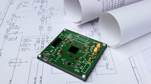
理想的PCB设计始于发现需要PCB的发现,并继续通过最终生产板(Fig. 1)。在确定为什么需要PCB,亲duct’s final concept should be decided. The concept includes the design’s features, the functions the PCB must have and perform, interconnection with other circuits, placement, and the approximate final dimensions.
环境温度范围和有关操作环境的疑虑应解决,并用于指定为PCB选择的材料。必须选择组件和PCB材料,以确保在所有预期的胁迫和潜在胁迫形式下运行板在其一生中可能会暴露于其。
电路示意图是根据概念绘制的。该详细图显示了PCB每个功能的电气实现。通过绘制示意图,应完成针对每个电路示意图的区域(由于电气原因或约束而密切连接的组件组),应完成最终PCB尺寸的现实图。
与原理图的创建同时,应生成材料清单(BOM)。电路中的组件应通过在考虑公差标准的同时分析电路每个节点的最大工作电压和电流水平来选择。通过选择电气满意的组件,应根据可用性,预算和尺寸重新考虑每个组件。
BOM必须始终与原理图保持最新。BOM需要每个组件的数量,参考指定器,值(欧姆,法拉德等数值),制造商零件号和PCB足迹。
These five requirements are critical because they define how many of each part are needed, explain identification and circuit locations while exactly describing each circuit element used for purchasing and substitution, and explain the size of each part for area estimations. Additional descriptions may be added, but it should be a condensed list describing each circuit element, and too much information can over-complicate library development and management.
PCB的文档应包括硬件尺寸图,原理图,BOM,布局文件,组件放置文件,汇编图纸和指令以及Gerber文件集。用户指南也很有用,但不需要。Gerber文件集是PCB术语,用于PCB制造商使用PCB的布局输出文件。一组完整的Gerber文件包括从板布局文件生成的输出文件:
- Silkscreen top and bottom
- 焊接顶部和底部
- All metal layers
- Paste mask top and bottom
- Component map (X-Y coordinates)
- 组装图顶和底部
- Drill file
- Drill legend
- FAB大纲(尺寸,特殊功能)
- NetList文件
Fab大纲中包含的特殊功能包括但不限于凹口,切口,斜角,充满底线的vias in-pad(用于设备下有各种销钉的BGA型IC包),盲/掩埋VIA,表面饰面和水平,孔公差,层计数等。1
示意图控制项目,因此准确性和完整性对于成功至关重要。它们包括适当操作电路所必需的信息。示意图应包括足够的设计详细信息,例如引脚号,名称,组件值和评分(Fig. 2)。
嵌入每个原理图中的符号是用于确定价格和规格的制造商零件编号。包装规范确定每个组件的足迹大小。第一步应该是确保每个引脚的裸露铜在适当的位置,并且根据可用区域和焊接方法的不同,并且比组件引脚(3至20 mils)大。
Consider assembly when designing footprints, and follow the manufacturer’s recommended PCB footprint. Some components come in microscopic packages and do not allow room for extra copper. Even in these cases, a stripe of 2.5 to 3 mils of solder mask should be applied between every pin on the board.
Follow the rule of 10. Small vias have a finished hole size of 10 mils with 10 additional mils of pad ring. Traces should be 10 mils or further from the edge of the board. Trace-to-trace pitch is 10 mils (5-mil air-gap, 5-mil trace width, 1-oz copper). Vias with 40-mil diameter holes or larger should have a pad ring added for reliability. An additional 15 to 25 mils of clearance beyond the design rule should be instated for copper planes on outer layers from plane to pins. This reduces the risk of solder bridging at all solder points.
组件放置在此过程中是下一个,并基于热管理,功能和电噪声注意事项确定。在分配了组件和互连位置的概述之后,首次组件放置步骤开始。放置各个组件后,应立即进行安置审查,并进行调整以促进路由和优化性能。
放置和包装尺寸通常会重新考虑,并根据尺寸和成本进行更改。吸收超过10 MW或进行10 mA的组件应被认为足以在热量和电气考虑方面强大。敏感的信号应用平面屏蔽噪声源,并保持阻抗控制。
力量management components should utilize ground planes or power planes for heat flow. Make high-current connections according to the acceptable voltage drop for the connection. Layer transitions for high current paths should be made with two to four vias at each layer transition.Place multiple vias at layer transitions to increase reliability, reduce resistive and inductive losses, and improve thermal conductivity.
The heat generated by the IC is transferred from the device to the copper layers of the PCB(Fig. 3)。The ideal thermal design will result in the entire board being the same temperature. The copper thickness, number of layers, continuity of thermal paths, and board area will have a direct impact on the operating temperature of components.
为了轻松降低工作温度,请使用更多的固体地面或电源平面直接连接到具有多重VIA的热源。建立有效的热量和高电流路线将通过对流优化传热。通过最大化用于热传递到大气的区域,使用热导电平面均匀地散布热量可大大降低温度(图4)。2
随着热分布,以下公式可用于估计表面温度:
p =(热量对流)x区域x(ΔT)
在哪里:
p =板上消散的电力
Area = board (X axis x Y axis)
ΔT=表面温度 - 环境温度
Heat对流= convection constant based on ambient conditions
Fine-Tuning The Component Placement
Components should be placed in the following order: connectors, power circuits, sensitive and precision circuits, critical circuit components, and then the rest. The schematic is built around each part on the PCB and completely interconnected. Routing priority for the circuit is chosen based on power levels, noise susceptibility, or generation and routing capability.
In general, trace widths of 10 to 20 mils are used for traces carrying 10 to 20 mA and 5 to 8 mils for traces carrying less current than 10 mA. High-frequency (greater than 3 MHz) and rapidly changing signals should be carefully considered when routed along with high-impedance nodes.
The lead engineer/designer should review the layout, and physical locations and routing paths should be adjusted iteratively until the circuit is optimized for all design constraints. The number of layers depends on power levels and complexity. Add layers in pairs since the copper cladding is produced that way. The routing of power signals and planes, the grounding scheme, and the board’s ability to be used as intended all influence operation.
最终检查应涉及验证敏感的节点和电路适当地避免噪音源,销钉和VIA之间存在焊料面膜,丝网印象清晰明确。在确定层堆叠时,请使用组件侧以下方的第一个内层作为地面,并将功率平面分配给其他层。堆叠是以平衡板相对于Z轴中点的方式创建的。
Consider any concerns the PCB designer has during the reviews, and correct the PCB based on feedback generated by the reviews. Create and verify lists of changes during each review iteration until the board is finalized. During all stages of the layout, keep the design error free by using the design rule checker (DRC).
刚果民主共和国只能捕获已编程以监视的错误,而刚果民主共和国规则集通常会根据单个设计而更改。至少,设计规则检查应涵盖包装到包装间距,无连接的网(识别电路节点的每个节点的唯一名称),短网,违反气隙,如果Vias离焊接太近,则彼此之间太近,违反垂直清除。
Many other important DRC rules can be set to ensure a robust design, and they should be researched and understood. For example, keep clearances at or above 5 mils. Vias should not be located within surface-mount pads (unless back-filled). And, solder mask should be between all solder points.
成本通常是PCB设计背后的驱动影响,因此最好了解PCB制造中的成本增加。一个典型的板是两到四层,没有直径小于10万的钻孔和最小气隙和痕量宽度。它的厚度也应为0.062英寸,标准FR-4,铜箔重量为1盎司。其他层,额外厚或薄的板,pad中的VIAS,后填充vias(由于电导率限制和热膨胀差异而首选),盲/掩埋vias以及交货时间都大大增加了整体成本。
Manufacturer capabilities should be understood when the PCB design commences. PCB fabs are routinely contacted about capabilities and cost reduction techniques when designing PCBs for manufacturability.
PCB设计可能很复杂,但是很有可能用一些技巧和练习来设计好板。使用这些准则并在需要时添加研究,经验丰富的退伍军人可能会继续磨练自己的技能,新手设计师可能会学会创建超出预期的高质量PCB。
1. Cohen,Patricio,Concepts and terminology used in Printed Circuit Boards (PCB), Electrosoft Engineering, Web, May 25, 2013.
2. Mauney, Charles,表面安装布局的热考虑, Texas Instruments, Web, May 13, 2013.